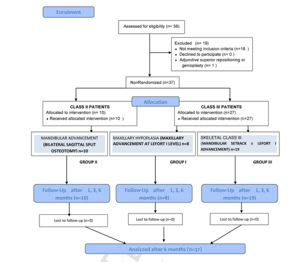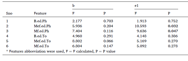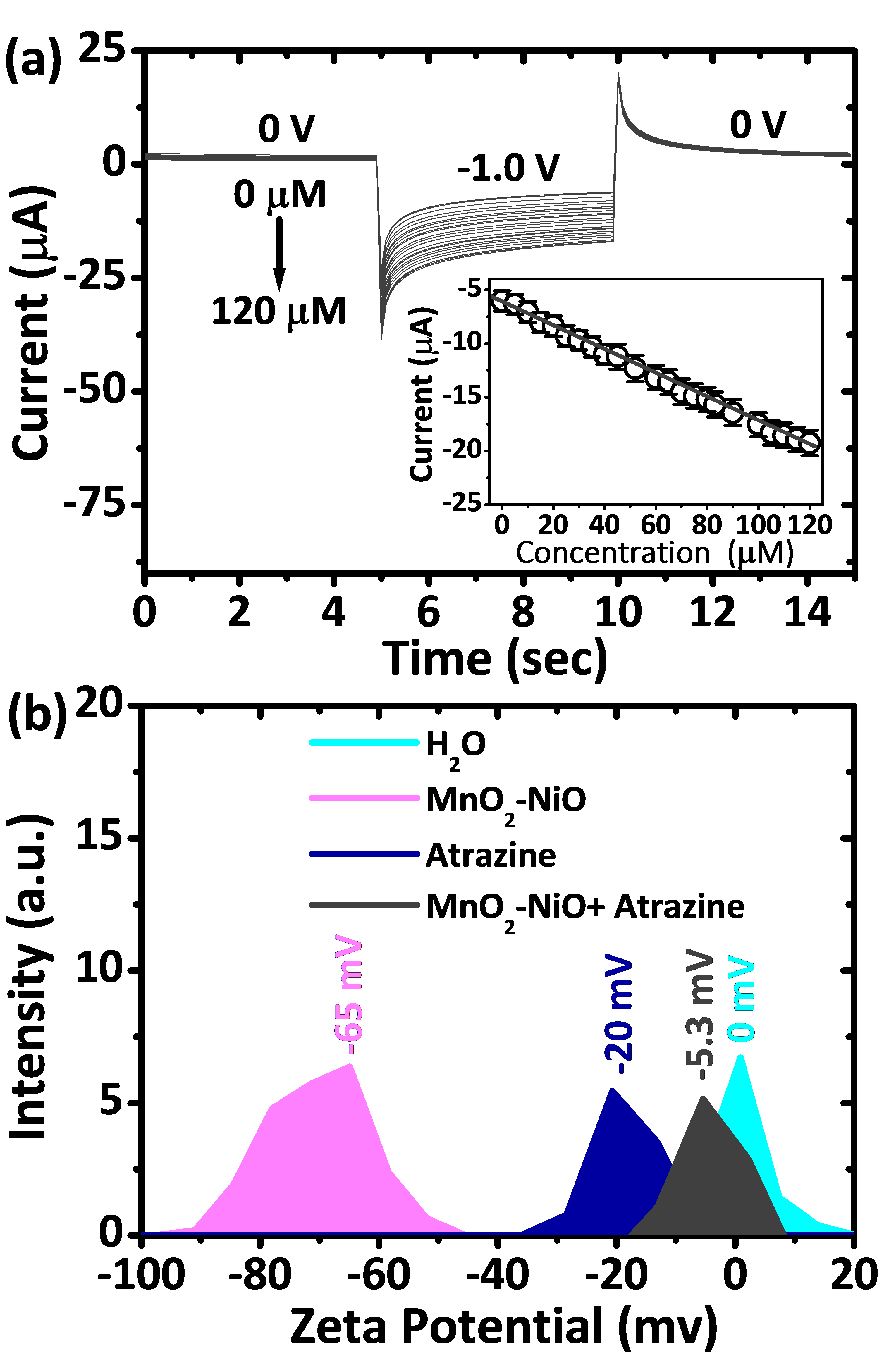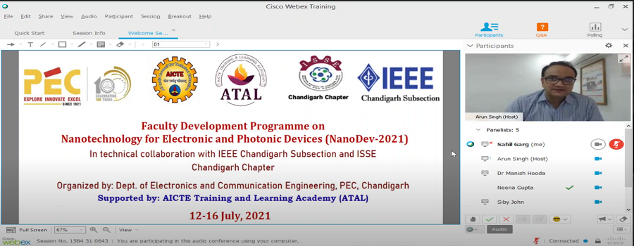
An online ATAL Faculty Development Programme On Nanotechnology for Electronic and Photonic Devices (NanoDev-2021) has been organized by department of Electronics and Communication Engineering, Punjab Engineering College (Deemed to be University), Chandigarh in technical collaboration with IEEE Chandigarh Subsection and Indian Society of Systems for Science and Engineering (ISSE) Chandigarh Chapter from July 12-16, 2021. Two Hundred participants from various Universities, Research organizations and Industries registered for the course. The event was coordinated by Dr. Arun Kumar Singh with an objective to provide an insight to understand and utilize the unique properties and interaction of novel materials, their physics and chemistry for the design and development of state-of-the art next generation electronic and photonic devices to meet the needs of relevant industry, space, defense and research organization. The FDP “NanoDev-2021” was funded by All India Council for Technical Education (AICTE) under its AICTE TRAINING AND LEARNING (ATAL) ACADEMY programme.
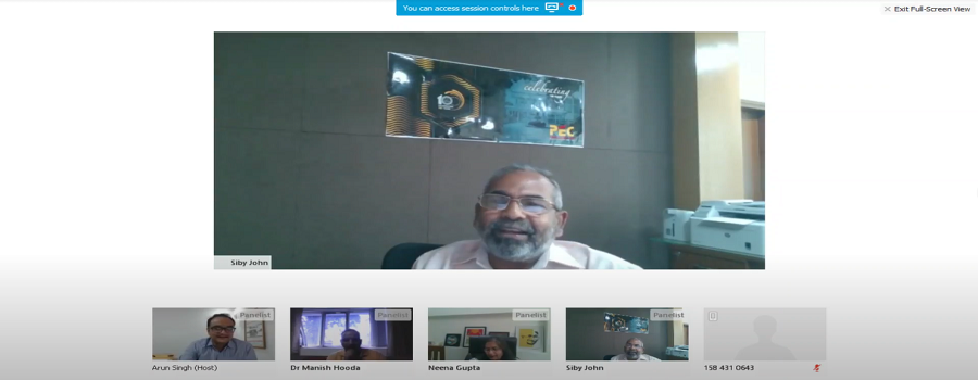
The event was inaugurated by Prof. Siby John, Director, PEC in the presence of Prof. Neena Gupta, Head, Dept. of Electronics and Communication Engineering, Dr. Manish Hooda, Scientist SCL Mohali and Secretary, ISSE Chandigarh Chapter. Prof. John appreciated the efforts of Course coordinator to rope-in eminent speakers from leading research universities, defense and space laboratories and industries to deliver talks on different nano-electronic and photonic technologies. He further encouraged the participants for responsible development of products based upon such technologies to meet out the most pressing human and societal needs.
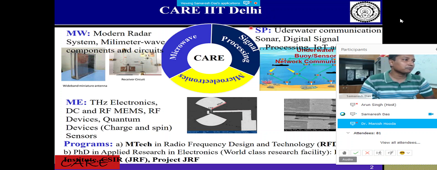
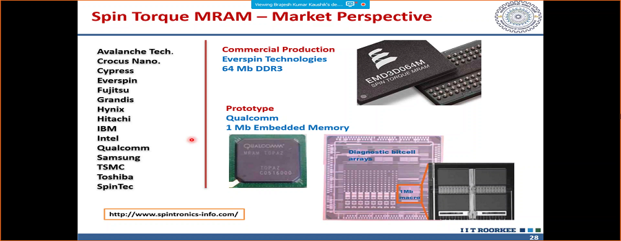
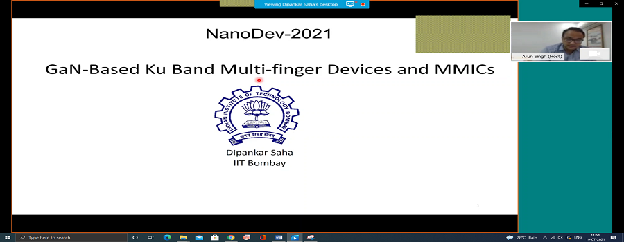
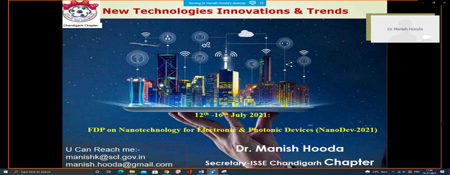
In the inaugural talk on day 1, Dr. Manish Hooda, Sr. Scientist, of Semiconductor laboratory (SCL) Mohali emphasized the new technology innovation and trends particularly miniaturization of devices and its advantages to the semiconductor industries. Prof. Dipankar (IIT, Bombay) introduced GaN-Based Ku Band Multifinger Devices and MMICs. In this, he emphasizes the GaN materials over others and elaborated GaN HEMT fabrication techniques and their application. Dr. Brajesh Kaushik, IIT, Roorkee introduced on Spintronics-Perspectives and Challenges. He talks about the fundamental of Spintronics and different types of memories with their hierarchy. In the last lecture of day 1, Prof. Samaresh Das (IIT Delhi) discussed nanodevices for silicon quantum computing. Further, he elaborated on the realization of the quantum computer, single-atom transistor, silicon quantum information technology, semiconductor metal oxide quantum dot, and silicon quantum information technology.
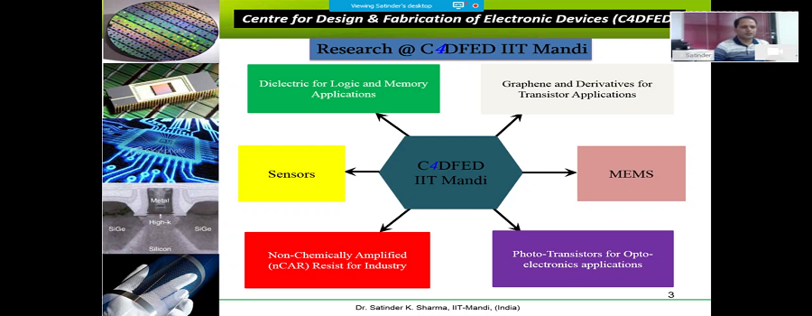
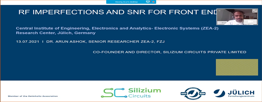
On day 2, Rahul K Sharma (SCL Mohali) explained the effect of optical parameters on the design of highly reflecting distributed Bragg reflectors (DBRS) for space applications. Next, the talk was delivered by Dr. Arun Ashok, Central Institute of Engineering, Electronics and Analytics Research Centre (ZEA), Jellich, Germany discussed RF Imperfections and SNR for Front Ends. He first introduced the various research activities being carried out at Julich Research Center. Thereafter, he discussed the receiver input scenario, impairment to the dynamic range (DR), receiver noise figure, Friss equation, Phase noise from the synthesizer, impact of non-linearity, and PLL noise in detail. In the closing lecture, Satinder K Sharma (IIT Mandi) discussed the next generation resist technology for semiconductor Fab-line. He started with a brief introduction to semiconductor technology advancement, then discussed the next generation lithography roadmap followed by lithography techniques. Further, He explained the resist technology roadmap for high volume chip manufacturing with EUV Resist developed at IIT Mandi.
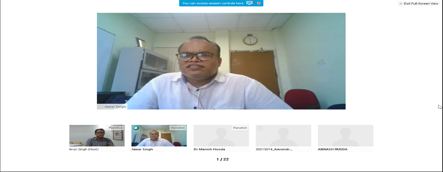
On day 3 of the workshop, the first talk was delivered by Jawar Singh (IIT Patna) on semiconductor devices and circuits for brain-inspired computing. Further, he elaborated on the motivation of alternative computing approaches, and why neuromorphic/ In-memory computing is used? He further elaborated about the advantages of in-memory computing over that of traditional computing, elements of in-memory computing, energy efficiency for AL and ML applications. Prof. Santanu Mahapatra, Indian Institute of Sciences (IISc) Bengaluru explained the Insights to two-dimensional non-volatile resistive memory devices. He discussed Von-Neumann architecture, In-memory computing, memristors, 2D material-based resistive switching devices, and atomristor. He concluded the session with a discussion on Resistive switching in monolayer MoS2. In the last lecture of day 3, Lokesh Pandey (Art of Living), conversed about different breathing techniques, raising energy level through breathing and meditation, and how the increase in energy level removes all negativity from life. He also carried out a short meditation and exercise session which aimed to relax the participants from the stress of daily life.
On day 4 of the workshop, the first talk was delivered by Dr. D. S. Rawal, Scientist, Solid State Physics Laboratory (SSPL), DRDO in which he introduced GaN-based HEMT Technology for Microwave Applications. In this, he talks about the technique to enhance output power and the cause of device degradation. He also talks about recent developments in GaN HEMTs technology and its market forecast. Dr. Meena Mishra, Scientist, SSPL. Delhi talked about RF characterization of GaN high-power devices and circuits. She started her talk by apprising everyone about various measurement facilities for S-parameters, pulsed, noise, and power measurements. She further discussed the role and importance of characterization such as in detections of traps in GaN HEMTs. In the last lecture of day 4, Dr. Jaspreet Singh, a Scientist at SCL Mohali discussed microsystem manufacturing. In this, he introduced MEMS fabrication technology and its derivatives and also talked about its application.
The first talk on the last day of ATAL FDP was delivered by Mr. Ayan Karmakar (SCL Mohali) on Silicon RF (Si-RF) Technology: Its Relevance to Modern Era Communication. He started with how silicon on-board shifted to silicon on-chip and also talk about different losses to the Silicon substrate in RF application. Mr. Nitin Sharma, ST Microelectronics, Noida talked about Generic Memory Architecture and Testing Challenges in Sub Nanometres Technology. He further discussed about the memory architecture, memory function, and fault specific to memory, and also elaborated the approach and solutions.
The event was concluded with a virtual training session of Silvaco TCAD device simulation software by Mr. Sahil Garg, JRF at PEC, Chandigarh and a virtual tour of upcoming cleanroom facility at the Department of ECE, PEC, Chandigarh. A feedback session was also held in which participants expressed their views and showed great satisfaction at the successful completion of the NanoDev 2021. Participants also suggested conducting such FDP in nanotechnology as exposure to these upcoming technological innovations in electronic and photonic systems is highly enlightening particularly for the younger researchers and is the need of the hour. This year’s FDP offered a wide range of lectures in the nano-electronics and nano-photonics domain, including materials for nanodevices, novel nano-electronic devices for microwave rectification, plasmonic-based devices, MMICs, and device fabrication techniques, HEMT devices and characterization techniques, memory devices, MEMS and their simulation techniques said Dr. Arun Kumar Singh, Coordinator, NanoDev 2021. He thanked all the invited speakers for sharing their research experiences with the participants and acknowledged the full support of Prof. Siby John, Director, PEC, and Prof. Neena Gupta, Head, Dept. of Electronics and Communication Engineering in the organization of FDP. He further showed gratitude to Dr. Manish Hooda, Scientist SCL Mohali and Secretary, ISSE Chandigarh Chapter for technical collaboration and AICTE for financial support.