


Comparative analysis of radiation tolerant analog circuit layout in 180 nm CMOS technology for space application
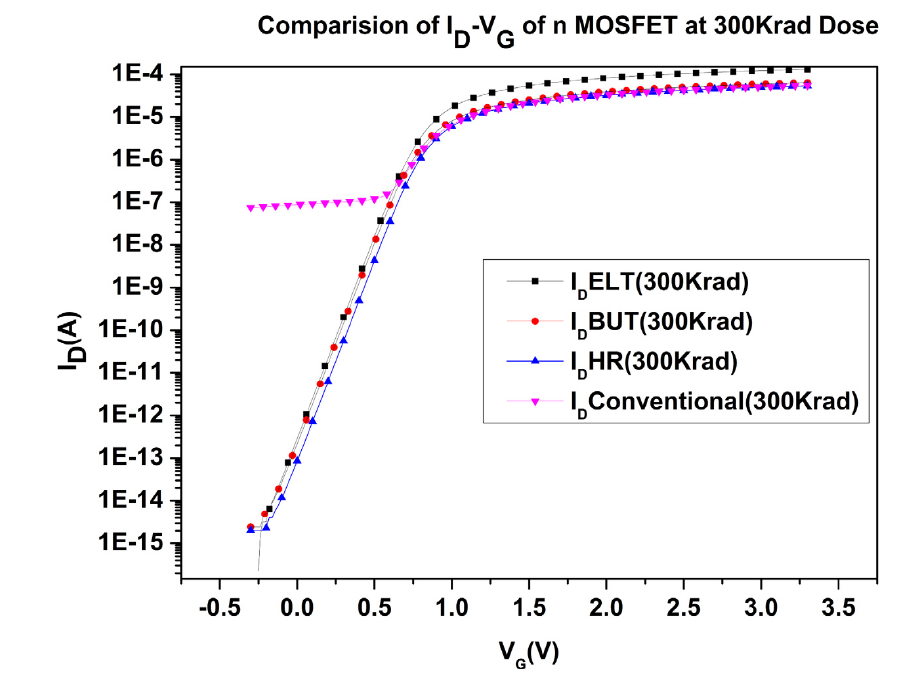
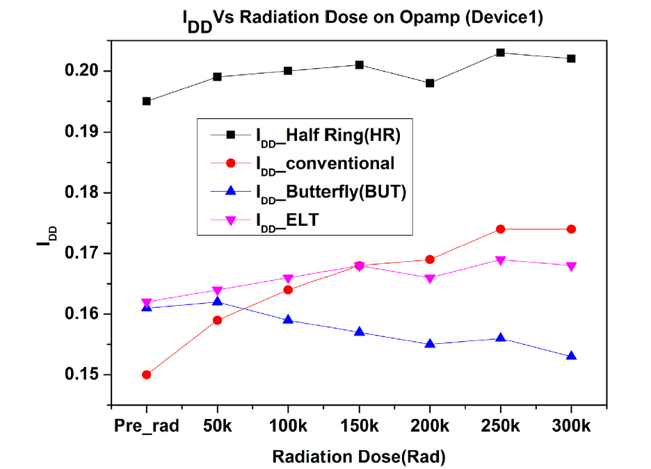
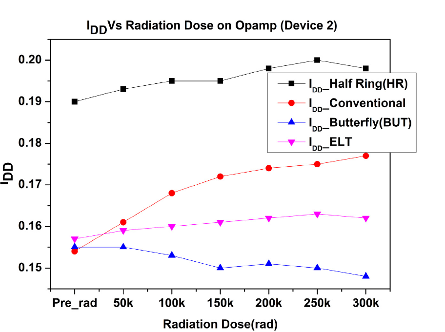
| Abstract | This work extend the application of radiation hard by design(RHBD) techniques to circuit level and review the effectiveness of these methods based on performance of analog domain circuit in radiation environment. A 3D TCAD tool was used in simulating the different layout styles of NMOS device. The parameter like Ioÿ (off state leakage current), Ion(on state current), Vdsat( saturation voltage), Vth (threshold voltage), Ro (output resistance) and gm(trans-conductance) were in focus. A test chip comprising of four opamp circuits and implemented using different layout method(conventional, Half ring, Butterfly, ELT) . The test chip was fabricated in SCL’s 180 nm process and total ionization dose(TID) tolerance testing up to 300K rad was done. The findings of the work as follows: half ring and butterfly layout styles perform at par with ELT in TID tolerance test. The bandwidth and slew rate metrics of opamp employing half ring and butterfly layout were better by 25% and offer better trade-off in terms of silicon area. The quiescent current in opamp circuit implemented with RHBD technique increases by 3% but 16% increment observed for opamp circuit implemented with conventional method for radiation dose of 300K rad. The presented work can provide insights to designers for selecting the RHBD techniques for rad hard application specific integrated circuit (ASIC) design for space/defense applications. |
| Faculty |
Prof. Neelam Rup Prakash
|
|
neelamrprakash@pec.edu.in
|
|
| Collaborations | Semiconductor Laboratory Mohali |
| More Information | https://doi.org/10.1016/j.mejo.2022.105665 |