


Novel GaN Self-Switching Diode Based Frequency Multipliers
| PI Details | Co-PI Details |
|---|---|
|
Dr. Arun Kumar Singh
Designation: Professor |
Dr. Sanjeev Kumar
Designation: Professor |
| Funding Agency | Project Cost |
|---|---|
| (SERB-DST) Science and Engineering Research Board, Department of Science & Technology, New Delhi. |
Rs. 60,31,808.00 Amount Received till date (in Rs.) Rs. 39,55,000.00 |
| Start Date | Completion Date | Status |
|---|---|---|
| 2022-12-27 | Ongoing |
Abstract
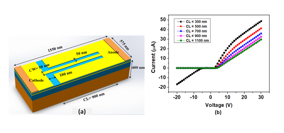
The Aim of this project is to design, develop and fabricate an integrated frequency multiplier utilizing a novel self-switching diode (SSD) based on GaN two-dimensional heterostructures. The SSD has an entirely different working principal which does not require any p-n junction and /or Schottky barrier to operate eliminating the requirement of an additional bias circuit than that of conventional and commercially available diodes. Due to planar and single-layered device architecture, SSD exhibits low parasitics resulting in a zero-bias rectification up to 1.5 THz at room temperatures with responsivity and NEP comparable to commercially available Schottky diodes. The SSD can easily be fabricated utilizing a single-step lithography followed by an etching process from using wide variety of materials varying from conventional Silicon to III-V heterostructures to novel graphene. On the other hand, commercially available Schottky barrier diodes, have multi-layered and vertical structure, and require an additional bias high enough to overcome the built-in electric field and to allow current flow. It further introduces the parasitic capacitance which in turn limits the operating speed and high frequency performance restricting to utilise a Schottky diode to generate very high microwave/ Terahertz frequencies. Schottky barrier diodes are commonly being utilised in array i.e. parallel or anti-parallel configuration for frequency multipliers to improve input/output power handling capacity. However, they suffer from excessive heat at the Schottky junctions leading to the performance degradation and require novel materials and challenging fabrication techniques to achieve ultra-low charge carrier transit time and parasitics at room temperature to generate high microwave/terahertz signals. Utilising excellent properties of GaN, SSD can be implemented for frequency multipliers to generate signals with hundreds of gigahertz frequencies with improved efficiency and high power handling capacity. Planar structure of device is more suitable as more number of SSDs in array configuration can be easily integrated without interconnects reducing overall device impedance exhibiting better noise properties at high frequencies. Further, heat dissipation can be managed efficiently by correct design of SSD channel. Therefore, developing GaN SSD based integrated frequency multiplier is timely given the rapid progress in the GaN technology and development of high frequency microwave/terahertz sources for wide variety of applications such as future generation communications, medical and security imaging etc. Additionally, training of early career researchers in this project will provide India with the scientists and engineers with the skills to transfer GaN-based technologies from academia to industry for industrial and/or strategic applications in line with Government of India’s Semiconductor Mission, Make in India, Aatmnirbhar Bharat, and Skill India Missions.
| Manpower Sanctioned/Hired | Manpower Trained |
|---|---|
|
JRF (Nos): 01 |
Ph.D Produced: 02 |
Equipment Sanctioned/Procured
|
Name of Equipment |
Make & Model |
Year of Purchase |
Cost (Rs.) |
Salient Features of Equipment |
Condition (Working /Not Working) |
|---|---|---|---|---|---|
|
Power meter with Sensors (50 MHz to 18 GHz) |
- |
- |
- |
Power Meter |
- |
|
Preamplifier (100 MHz- 26.5 GHz) |
- |
- |
- |
Pre Amplifier |
- |
|
RF Probes with Micropositioner |
- |
- |
- |
RF Probe |
- |
Publications
Output/Outcome of the Project