


Announcements
Home
Upcoming Programmes for Admission
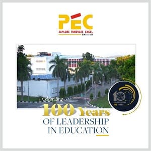 Centenary Celebrations
Centenary Celebrations
 Admissions
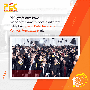 Academics
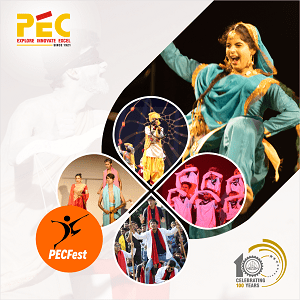 Student Life
Recent Research Activities


Agnipath Scheme

 Centenary Celebrations Admissions Academics Student Life


